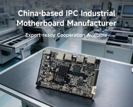

What is custom Android mainboard engineering?
Custom Android mainboard engineering converts a product requirement into a controlled hardware, firmware and manufacturing specification. The work should begin with interfaces, display, enclosure, power, environment, software and lifecycle requirements—not a processor shortlist.
Engineering stages
| Stage | Required output |
|---|---|
| Requirements | Use case, interfaces, environment and acceptance criteria |
| Architecture | SoC, memory, storage, power and connector plan |
| Hardware | Schematic, PCB, BOM and design review |
| Software | Boot, drivers, Android/Linux image and update method |
| Validation | Functional, thermal, EMC-precheck and endurance records |
| Release | Approved files, revision control and production test |
What information should the buyer provide?
Provide the target device, screen and touch panel, peripheral list, communication interfaces, mechanical limits, power source, operating temperature, target market, sample quantity and volume forecast.
How is engineering scope controlled?
Use a written requirement baseline and change log. Every prototype should identify the PCB revision, BOM version and firmware build so that a passed result can be reproduced in production.
Project enquiry: Send requirements to Androidsbc@163.com or call +86 132 6167 7119. Final specifications, certification scope, pricing and lead time are confirmed for the selected configuration.